logo
Datasheet4U.com - LC72700G
logo

LC72700G Datasheet, LSI, Sanyo Semicon Device

LC72700G Datasheet, LSI, Sanyo Semicon Device

LC72700G

datasheet Download (Size : 200.25KB)

LC72700G Datasheet
LC72700G

datasheet Download (Size : 200.25KB)

LC72700G Datasheet

LC72700G Features and benefits

LC72700G Features and benefits


* Delay detection scheme using a 1T delay
* Built-in error correction function using a 2T delay
* Digital PLL clock regeneration
* Block and frame synchr.

LC72700G Description

LC72700G Description

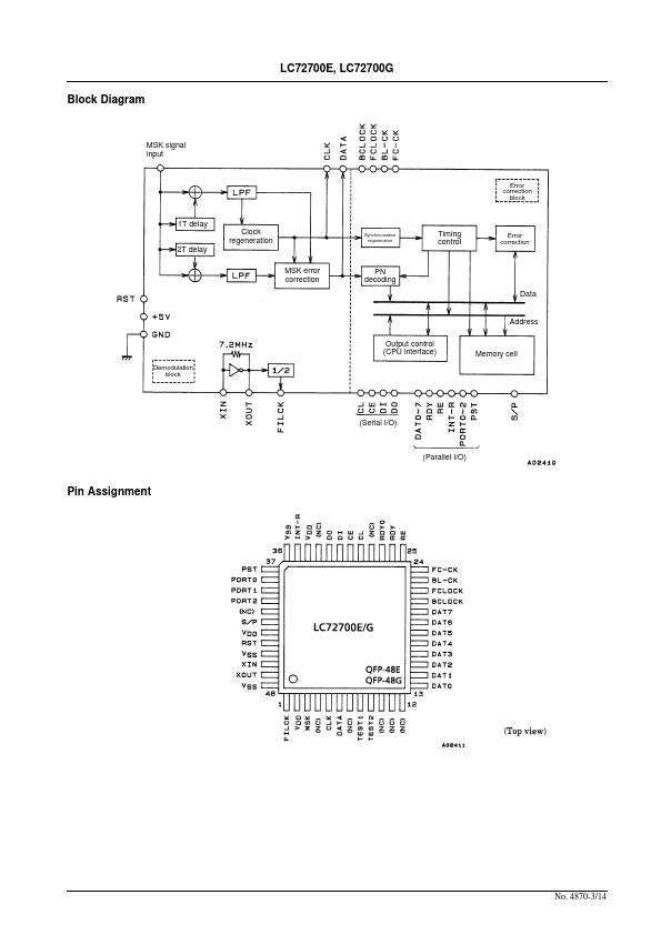
Pin No. 3 29 30 31 44 8 9 37 38 39 40 42 Symbol MSK CL CE DI RST TEST1 TEST2 PST PORT0 PORT1 PORT2 S/P 76 kHz MSK signal input CCB serial interface Clock input Data control input Data input Input System reset input pin (negative logic) Test pin 1 (n.

Image gallery

LC72700G Page 1 LC72700G Page 2 LC72700G Page 3

<?=LC72700G?> Page 2 <?=?> Page 3

TAGS

LC72700G
Mobile
Multiplex
Broadcast
Receiver
LSI
Sanyo Semicon Device

Manufacturer


Sanyo Semicon Device

Related datasheet

LC72700E

LC72701M

LC72705E

LC72706E

LC72707E

LC72708E

LC72709E

LC72709W

LC72710LW

LC72710W

LC72711LW

LC72711W

LC72714W

Since 2006. D4U Semicon.   |   Datasheet4U.com   |   Contact Us   |   Privacy Policy   |   Purchase of parts